What? Why?
What: The Zynq is a nifty chip (family of chips, I guess) from Xilinx that combines a couple ARM9 cores with some 7-series FPGA fabric. For a time it was one of the cheapest ways to bootstrap an ARM secure boot chain without minimum orders and NDAs.
Why: I missed out on the Switch hacking. It's complicated. Yes, I started this in 2018 and then put it down for 2 years.
Jumping in blind
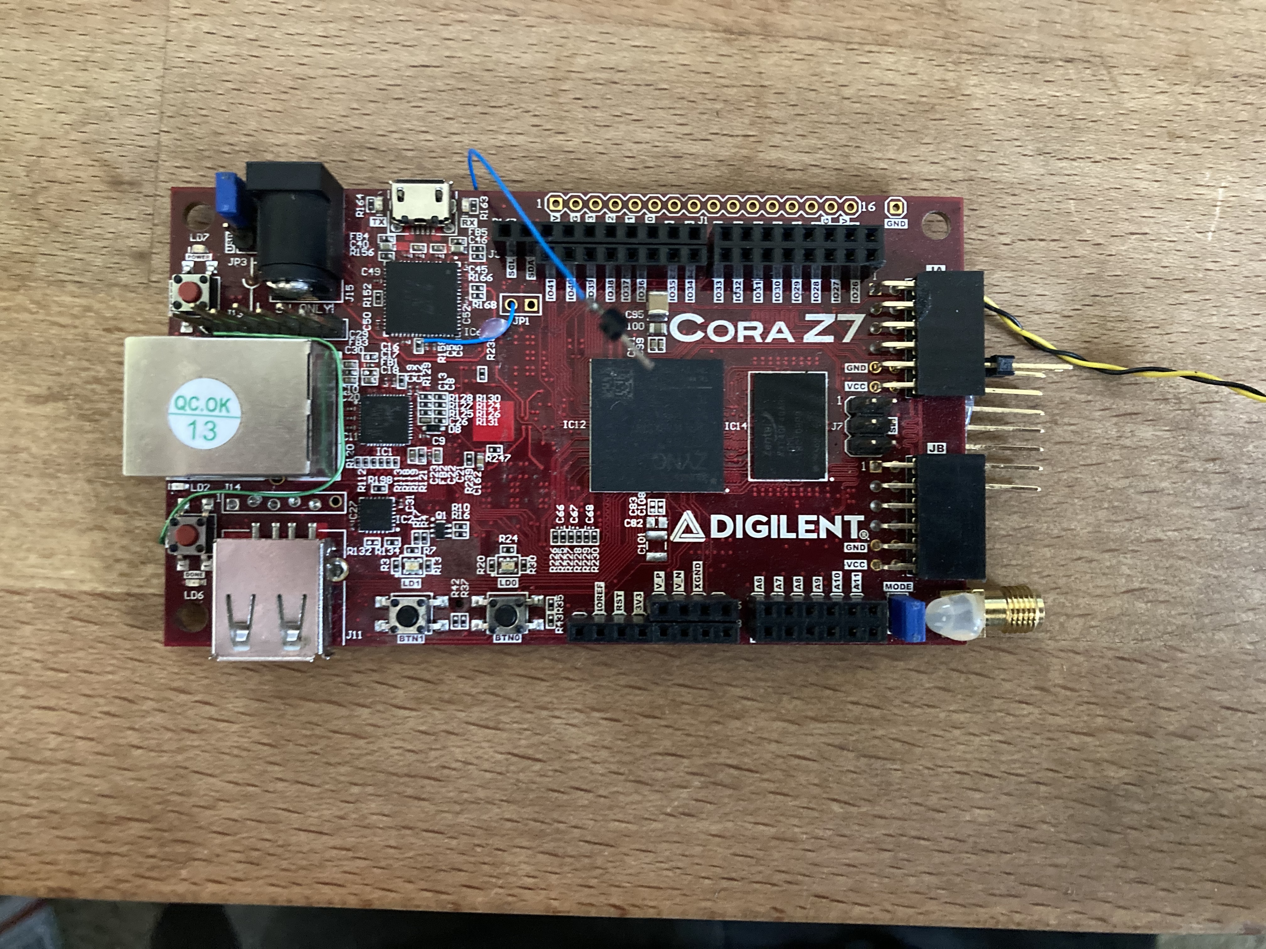
I picked up a Cora development board (one of the cheapest at the time) and poked around as much as I could immediately post-boot. My plan was to just gather as much information in the most unlocked state possible, and the pour over chip docs to look for interesting tidbits.
So I dumped all the register state immediately post-boot, then checked the On-Chip Memory (OCM) configuration and dumped those ranges as well.
I found around 512B of interesting code sitting at the very top of the OCM (0xFFFFFE00-0xFFFFFFFF). Here's the first basic block - I've annotated it with some of the register (and RAM) state in where they're relevant.
ROM:FFFFFE00  STR  R1, [R0]   ; 0xffffffff -> [0xf8007028] (disable ROM)
ROM:FFFFFE04  STR  R6, [R5]   ; 0x18-> [0xF8000910] ("OCM_CFG->SWAP" - remaps low OCM up by 0x30000 to make room for the ROM at 0)
ROM:FFFFFE08  DSB  SY
ROM:FFFFFE0C  ISB  SY         ; flush spec/readahead stuff, we just jumped to a stub in OCM
ROM:FFFFFE10  LDR  R11, [R4]  ; [RAM:0x0000] -> 0x9fa90ddc
ROM:FFFFFE14  STR  R9, [R4]   ; 0xe3e0f0d3 -> [??]
ROM:FFFFFE18  MOV  R12, #2
ROM:FFFFFE1C  STR  R12, [R10] ; 2 -> [0xf8000244] (assert CPU1 reset)
ROM:FFFFFE20  MOV  R12, #0
ROM:FFFFFE24  STR  R12, [R10] ; (deassert reset)
ROM:FFFFFE28  DSB  SY
ROM:FFFFFE2C  ISB  SY
ROM:FFFFFE30  STR  R11, [R4]
ROM:FFFFFE34  DSB  SY
ROM:FFFFFE38  ISB  SY
ROM:FFFFFE3C  MOV  R4, #bootmode
ROM:FFFFFE40  LDR  R7, [R4]
ROM:FFFFFE44  CMP  R7, #8
ROM:FFFFFE48  BEQ  loc_FFFFFE54
The rest of the disassembly isn't quite worth including inline (and it's easy enough to go dump yourself).
Assuming nothing else perturbed there registers, the visible code appears to just write to 0xf8007028 ("PCAP ROM SHADOW CTRL", according to some headers in the reference FSBL)
and then jump to LR. In my case, this was pointing to another tiny stub which just stuck both cores in wfe loops, while core 0 polled 0xFFFFFFF0 for an address to jump to.
When I was tracking down how the OCM was mapped, I noted a weird value in OCM_CFG - bit 3 clearly mapped in some additional OCM, or changed the mappings in some undocumented fashion.
I never figured out exactly what was going on before reversing the ROM, but this moved the OCM from its "low" position to just above the ROM. From my notes (not all correct):
OCM_CFG->SWAP appears to map OCM ROM in at 0x30000 (originally 0xffff0000 ?)

xsct% mrd 0x30000
Memory read error at 0x30000. OCM is not enabled at 0x00030000. Invalid address
xsct% mrd 0xF8000910
F8000910:   00000018

xsct% mwr 0xF8000910 0x10
xsct% mrd 0x30000
30000:   00000000
Basically, there is a third OCM location starting at 0x40000 in order to make room for the ROM. This becomes apparant reasonably quickly later, while reversing.
At this point I'd read enough of the TRM to get a good sense of how everything was glued together, and figured it would be about as easy to start glitching as it would be to try and find a logic bug (amusingly - there is one, kind of! It comes up later).
"Real Work"
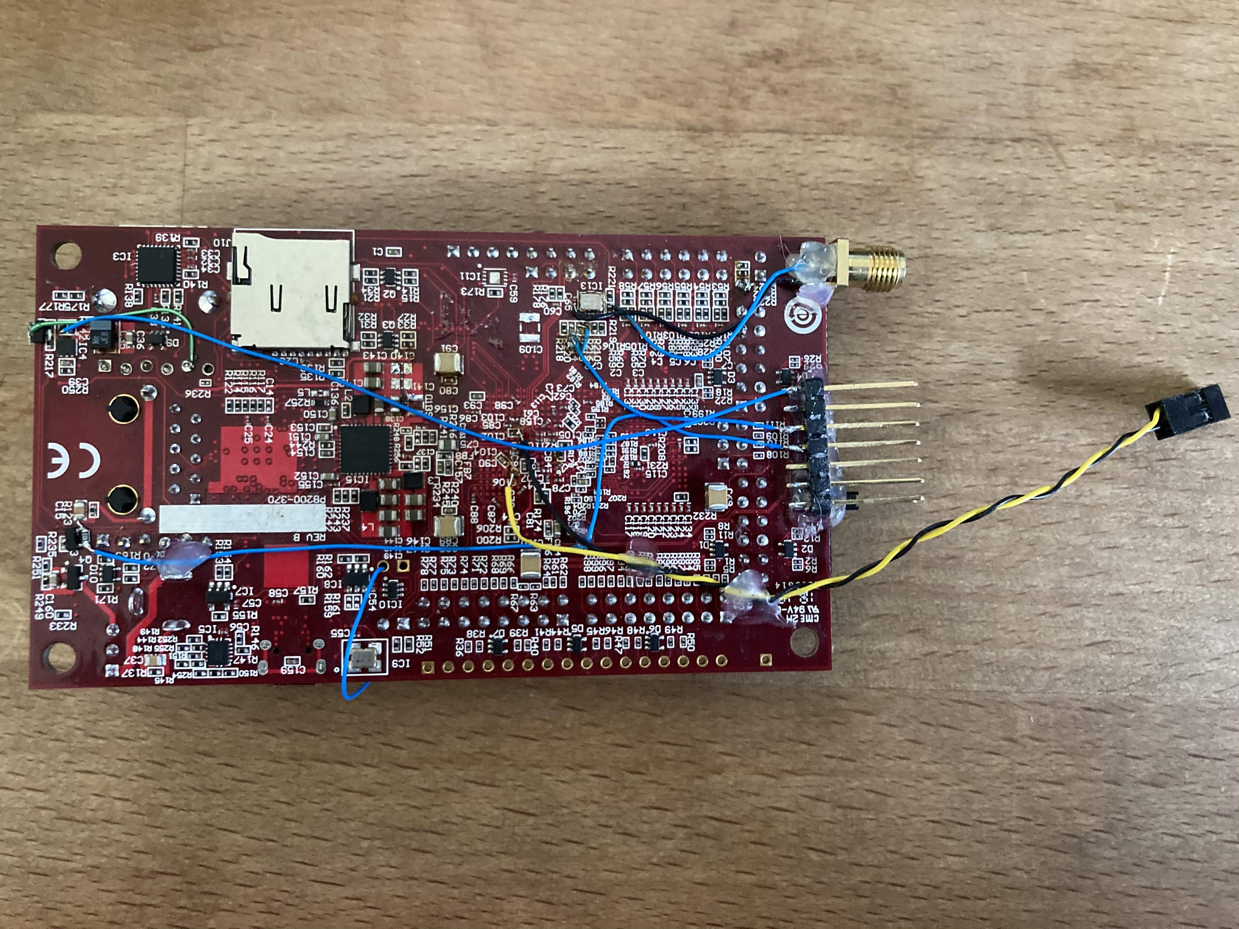
I made some modifications to the Cora, and before going further tested a trivial crowbar setup (SOT23 packaged FET across an old decoupling footprint :)). Once that worked, I removed the rest of the vccint caps, the inductor for the vccint rail smps phase, strapped the PLL_DISABLE pin, and exposed various clocks, resets, and gpio. For reasons I don't recall, I wanted something a little cleaner, so I copied Scanlime's homework, made some small edits, and laid it out in a PMOD-ish board (Oshpark, KiCAD).
Trigging the glitch was a whole different story: The Cora doesn't even route out sufficient MIOs to use SPI boot, and POR (Power-On Reset) wasn't sufficiently deterministic for what I needed... so I decided the best move at the time1 was to up and write an SDIO/MMC trigger (source published, uh, maybe never - it's not pretty).
To test the determinism, I wrote added some code that pulled a GPIO lane right at _boot (skipping as much non-determinism in the startup code!):
_prestart:
_boot:
// unlock slcr, enable + pull gpio 0.6 low, lock slcr

ldr     r0,=SLCRUnlockReg               /* Load SLCR base address base + unlock register */
ldr     r1,=SLCRUnlockKey               /* set unlock key */
str     r1, [r0]                        /* Unlock SLCR */

// set pin 6 direction
// 0xE000A204 <- 0x40
ldr r0,=XGPIOPS_DIRM
ldr r1, [r0]
orr r1,r1,#0x40
str r1,[r0]

// set pin 6 output enable
// 0xE000A208 <- 0x40
ldr r0,=XGPIOPS_OEN
ldr r1, [r0]
orr r1,r1,#0x40
str r1,[r0]

// set pin 6 configuration (drive, etc)
// 0xF800071C <- 0x600
ldr r0,=GPIO_PIN_CFG
ldr r1,=GPIO_CFG
str r1,[r0]

// set output data to 0
// 0xE000A040 <- 0
ldr r0,=XGPIOPS_DATA
ldr r1,[r0]
bic r1,r1,#0x40
str r1,[r0]

ldr r0,=SLCRlockReg             /* Load SLCR base address base + lock register */
ldr r1,=SLCRlockKey             /* set lock key */
str r1, [r0]                    /* lock SLCR */
And it was awful:
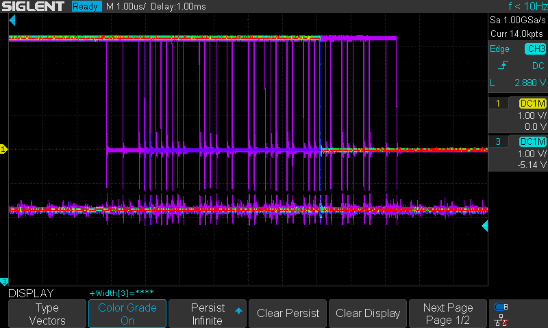 |
|---|
| ch3: sdio trigger (edge offscreen). ch1: gpio from firmware (edge: yes) |
At this point, the next best option seemed to be keeping track of glitch timestamps backward - basically: I'd keep a set of desired timestamps. Pick one, attempt to land a glitch at that time. Record when the DUT boots, remove whatever timestamp actually hit from the set. Repeat. I put that idea aside for later, and decided to chase down more nondeterminism.
This went on for ages (it's actually why I put it down in 2018...).
Everything was already clocked from the same source, and I had already elimated all of the startup code I could - Time to look at the one unknown factor (well, other than the Zynq): the SD card.
One interesting bit about SDIO is that it's source-synchronous, while being clocked always by the host - Note the start bit immediately before the direction flag:
And actually off the wire, a CMD17 (read block) request/response pair looks like this:
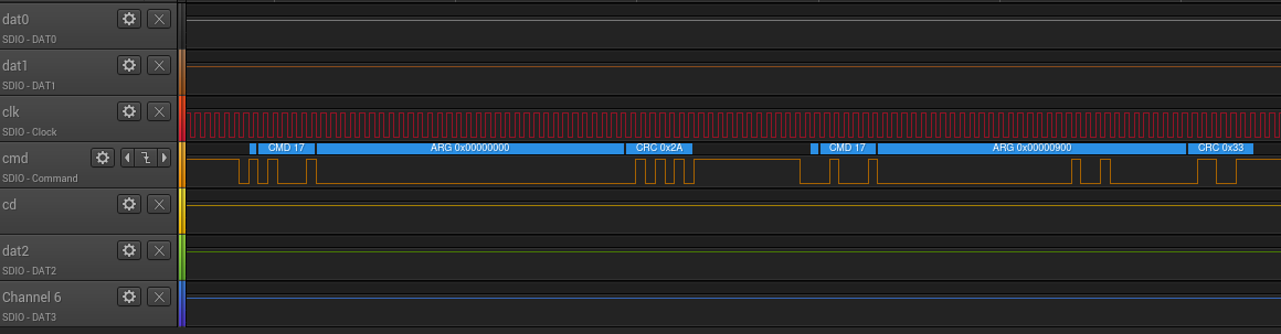
Realizing I had no idea what was going on in the junk-bin SD card I was using, I measured the delay between the host's query/command and the card's response: Of course, they varied wildly. I switched the triggering up to fire on the card's responses - and it got...a little better. Since SDIO is split across distinct data and command phases/lines, I tried triggering on the data response: another marginal improvement.
I began to think this was as good as I could reasonably get it, perfect was the enemy of good, etc etc - And I just wanted to see some wins. Jitter was low enough that I was willing to bet I could make up for it by repeating and/or overlapping test cases. To hopefully reduce the time it would take to reach the right spot, I ran the glitch range starting high (eyeballed with a scope and that same GPIO firmware), striding around 50% of the jitter range each test, and moving the glitch earlier each case. I set the repeat count to "enough" and let it run - and I started getting hits! As expected, it was super unreliable (like....20-40% once dialed in?) and still way too manual, but hey - It just needed to work once. Er, twice. The TRM lies about how big the ROM is.
I'm actually not sure where the last bits of nondeterminism came from - even having reversed some 80% of the bootrom. The Xilinx devs really liked sticking isb and dsb barries all over, so maybe those are nondeterministic due to the pipeline flushes?
But even that doesn't sound right...
I'd be very interested in hearing anyone's findings on this matter.
Finally - The Zynq BootROM has a "Register Init List" functionality - basically, you provide a list of tuples of (address, data), and if the address passes some checks (most of the fun things are removed...obviously this is massively impactful attack surface)
the write is done (wrapped in dmb). Instead of writing moderately obnoxious SDIO triggering code it's entirely possible just to use this list to poke a single GPIO. Probably even more deterministic. sigh.
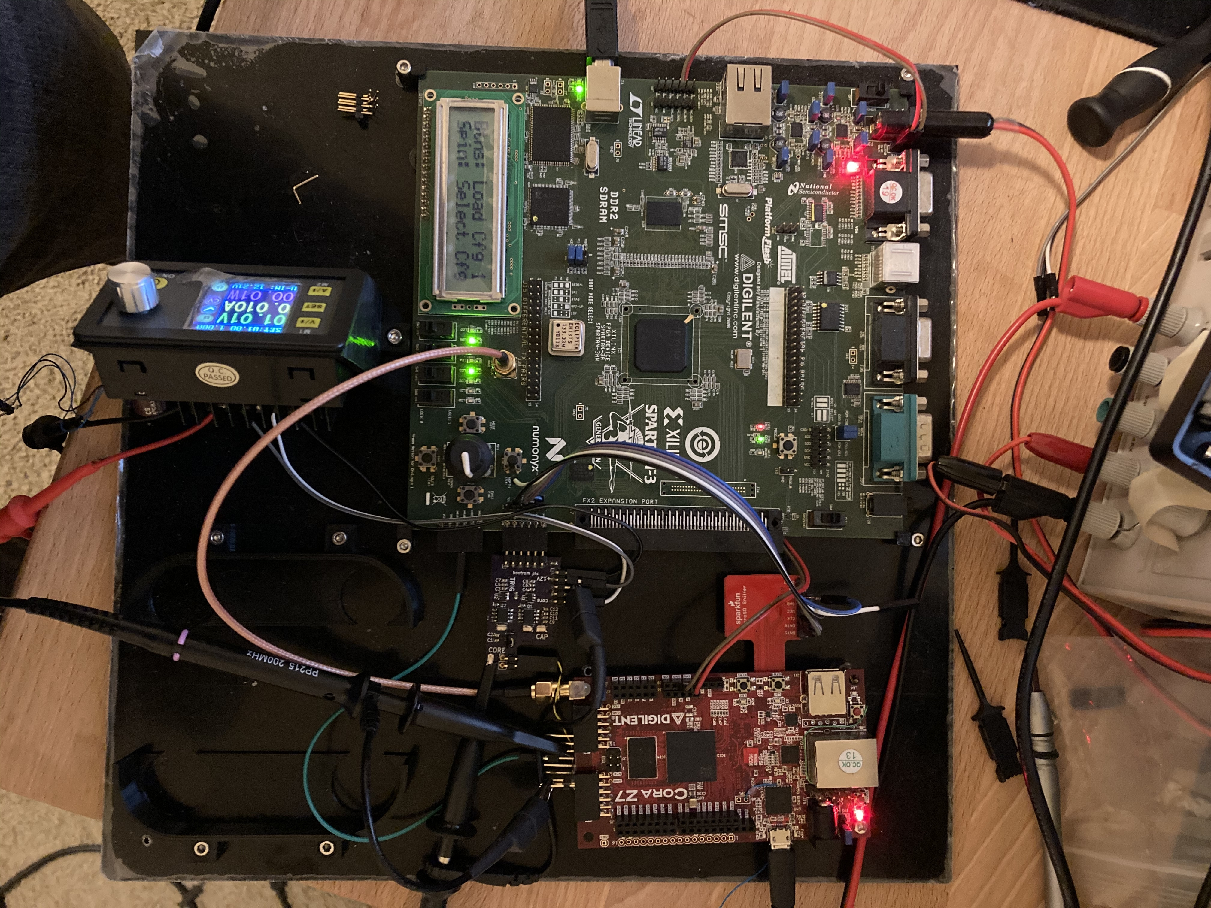
Unfortunately I didn't document as much as I thought I did beyond this point. The ancient Spartan-3A dev kit I was using kicked the bucket (dead SMPS, it'll get fixed when I fill a digikey cart...), so while that's a great sendoff for the board, I ended up modernizing the code and porting it to an Artx-7 board laying around. This makes for a better picture, though:
-
Forgetting all about the "Register Initialization Parameters" feature. See TRM table 6.7. ↩